©2026 Business Next Media Corp. All Rights Reserved. No.102, Guangfu S. Rd., Da'an Dist., Taipei City 106, Taiwan
The Amazing, humble silicon wafer
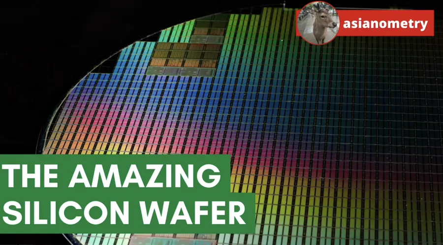
In this video, we are going to talk about the decades of research and stunning engineering that have gone into creating today’s cutting-edge semiconductor wafers.
Silicon is probably the single most studied element on earth. Over the past seventy years, people have researched more ways to cut it, etch it, grind it, clean it, crystallize it, polish it than almost anything else.
Engineers have done amazing things to turn this plentiful shiny rock into the century’s most impactful piece of technology. And the wafer industry needs some love for those achievements.
So in this video, we are going to talk about the decades of research and stunning engineering that have gone into creating today’s cutting-edge semiconductor wafers.
Introducing the Wafer
The silicon wafer is the fundamental building block for semiconductors, micro electromechanical systems or MEMS, and solar cells. The wafer serves as the substrate for microelectronics devices built on top of it.
There are generally two types of silicon wafers: Those graded for producing solar cells and those for integrated circuits. The latter requires higher grades of purity than the former. Eleven 9's rather than six 9's. 99.9999 ... well, you get the idea.
The industry produces them in three general sizes - 150, 200, and 300 millimeters. About the size of a takeout pizza. The larger the wafers, the more challenging they are to produce.
But if you make them right and with a good yield then bigger wafers are far more economical. But more on that later. Wafer manufacturing begins with the formation of a single, perfect silicon crystal or ingot. That perfect silicon crystal starts with the most pristine sand. Let us talk about it.
Wafer Sand and Silicon
Today's modern wafers are made from silicon, Earth's second most abundant element. Silicon itself is a blue-gray, brittle element in the same group as Germanium and carbon on the periodic table.
Silica is a major component of sand. So yes, almost all silicon wafers begin with sand. But it makes the most economic sense to source the purest possible natural sources of sand and save consumers the trouble of additional purification work.
Like all minerals and people, quartz is influenced by the environment in which it is grown. Impurities happen when trace elements or minerals enter the mineral as it grows. For instance, water or gas bubbles.
The single biggest source of high-purity quartz comes from the secretive Unimin Corporation in the United States, now known as Covia. They mine out of North Carolina, near the town of Spruce Pine. They process wafer sand out of pegmatite deposits.
There are other companies in the space. The biggest alternative supplier is the high quality quartz from Drag in Northern Norway. Their quartz is mined by Norwegian Crystallites.
Sand to Polysilicon
The purest wafer sand in the world currently available has a purity of 99.9992% - with trace elements of boron in quantities of 40 parts per billion. Most wafer sand is not like this. And even then, 3 nines of purity is still too dirty and disgusting for semiconductors.
So more purification work needs to be done. You take your wafer sand - which is often far short of 99.9992% - and mix in a carbon source like coke, coal or wood chips. Then you heat it in a submerged electrode arc furnace to temperatures from 1500 to 2000 degrees Celsius.
Silica is silicon dioxide. So when you add carbon and energy to it, the oxygen leaves the silicon and attaches itself to the carbon.
What you have at the end of it is something called metallurgical-grade silicon or MG-Si, with a purity grade of 98-99%.
98% is pretty good if you just took a midterm, but it falls far short of semiconductor-grade silicon. So you need to purify it even more.
You take the powdered metallurgical silicon, add hydrochloric acid, and throw it in a reactor heated to 300 degrees Celsius. They react together to create a new set of intermediate chemicals. These we can then process into semiconductor-grade polysilicon. These chemicals can vary but technicians have mostly chosen to try for trichlorosilane.
Making Semiconductor-grade Silicon
Throughout the process of creating trichlorosilane, the acid will scrape away traces of iron and aluminium. Once you have the pure trichlorosilane, it is vaporized and placed along with pure hydrogen into a chemical vapor deposition reactor.
There, the gas decomposes, depositing the silicon onto very thin rods of silicon called "slim rods". After about 200 to 300 hours of slow growth at 1100 degrees Celsius is a larger rod of semiconductor-grade polysilicon.
This method of using CVD to deposit silicon onto thin metal rods is referred to as the Siemens Method. Named after Siemens the company, which first patented it back in the 1950s.
There is also a competing process using fluid bed reactors which has been catching on lately due to its better economics. I mention it because the phrase "fluid bed" makes me think of water beds.
Solar Polysilicon
The Siemens method gives you your desired purity. But you also only get back about 30% of the silicon you put in while consuming a lot of power. This is fine for semiconductors, but presents more challenges for the solar industry.
Solar-grade polysilicon does not have to be as pure as semiconductor-grade polysilicon. Furthermore, the solar cell industry is more competitive and cost-sensitive than the semiconductor industry.
Solar energy has to be market competitive with fossil fuels and wind, which means the panels have to cost as little as possible.
Thus it does not make financial sense to produce solar-grade polysilicon with processes so strict on purity. So a few companies have explored ways to process metallurgical silicon - which if you recall is only 98-99% pure - into something good enough for solar cells.
One way has been to leach acids onto this silicon. It has been good at taking out some impurities but falls short when it comes to others. The science here still needs more work. Anyway let us go back to semiconductor silicon.
Making Crystal
The next step en route to semiconductor wafers would be to create the crystals. Like always, the crystals have to be pure and free of defects or dislocations.
95% of the industry's crystals are grown using a process called the Czochralski method. I shall hereby refer to it as the CZ method because I don't want to go insane.
In 1916, Jan Czochralski, a Polish metallurgist working in Berlin, published a way of making single metal crystals. He discovered this accidentally, with his pen.
Let me do a primer for the Gen-Z members of my audience. Back then, they used these things called pens to write. You dip the pen into these things called inkwells to cover the pen's nib in ink. You then write on these things called paper.
Paper is like an iPad that doesn't run out of battery.
Anyway, Jan needed to reload his pen with ink so he moved to dip his pen into the inkwell. But he accidentally dipped it into a crucible of molten tin.
He pulled the pen out of the crucible and saw a tiny thread of solidified tin hanging from the pen's nib. He soon verified that this thread was a single, solid crystal - continuous and unbroken from edge to edge.
The first transistors were made of germanium. Scientists GK Teal and JB Little modified the original CZ method to create germanium crystals. So really, this should be called the Teal and Little method.
When the industry switched to using silicon, they brought the CZ method with them. Teal and Buehler started growing CZ silicon crystals in 1951.
The CZ Method
It is all one crystal, but it is grown in stages. And each stage requires differing conditions.
The CZ method starts with a pool of polysilicon melt in a quartz crucible. This is made by melting solid chunks at temperatures of 1,420 degrees Celsius. You have to keep the melt at a very high temperature to prevent the formation of air bubbles.
Then slowly, you introduce your seed crystal into the melt. This small thing is usually only about a few millimeters large and has the same shape as your final crystal.
You wait until a small portion of the seed starts to melt too. Then you pull the seed out of the melt while also twisting it. Repeat.
If done right, the melt will crystallize under the seed below the point of contact between the seed and the melt.
By controlling the rate of the pulling and the heat temperature, you grow the rest of the crystal. Including its conical and cylindrical parts.
As you approach the end of the crystal, you again create a tapering-off end-cone shape. This is to prevent the crystal from developing imperfections due to differing temperatures and unavoidable inconsistencies in the pulling technique.
Sidebar. I left so much out here about growing crystals with the CZ method. There’s books and books written about this single section. If you’re interested I highly recommend reading up on it.
The first silicon crystals were small and light enough to be handled by hand - about 8 inches long and 0.75 inches in diameter. Over time, they have gotten larger - to the point where they need special equipment for proper handling.
The CZ machines in the 1970s were about 14 feet high and weighed about 30-40 kilograms. Over the years, they have more than doubled in height and weigh in at over 400 kilograms.
Modern machines are equipped with heat shields, cameras, and magnetic fields to review and maintain quality control. Decades were spent researching and honing the method to get crystals as free as possible of impurities and dislocations.
Cutting and Sawing
Once the crystals are made, you need to cut them into wafers. This is nothing like slicing up a sausage. First, you cut off the crystal's crown and tail cones.
The body is sawed into different sections and ground down into ingots. Crystals are mostly grown larger than their specific dimensions so the extra needs to be ground down. Notches are then placed to tell the saw where to cut.
Now we saw.
There are two ways to saw the ingots. The first is a diamond inner diameter saw. What does that mean? Conventional saw blades are mounted at the center and have their cutting edges on the outside diameter. Inner diameter saws are the opposite.
They cut one wafer at a time and each cut takes a few minutes. As it is cutting, the blade might flex or have imperfections of its own. These cause wafer defects that need to be corrected later on.
The alternative is to use a wire. With early wire saws, the wire is not actually doing the cutting. What it actually does is transport a slurry of silicon carbide grit and oil to the ingot, and that does the cutting.
Recently, the industry has started to use diamond-abrasive wire saws. Steel wire coated with diamonds. It cuts faster while causing less damage to the wafer's overall structural integrity.
Wire saws take longer to cut a single ingot. But unlike the internal diameter saw, the wire saw can make all of its cuts at once. Due to this, wire saws have been preferred for wafers larger than 150 millimeters. The yields are better.
Note again, the concentration on yield, speed, and product quality. The semiconductor industry is not only a technical marvel, it is also a capitalist business. Plenty of methods are technically possible, but it has to also be financially better than whatever was done before in order to be adopted.
Polish and Finish
Ideally, once the wafers are cut out of the ingots they are ready to go. But in practice, there are imperfections. The wafer might have a warped shape. Their edges are rectangular, which makes it vulnerable to chipping. And their surfaces are contaminated with other substances.
So more work needs to be done to make sure you have the ideal wafer at the lowest cost. So next up is the lapping and etching stage. You remove any surface silicon cracked or traumatized by the wire cutting while maintaining the required flatness.
After this, you polish the wafer surface. You want to make sure that the wafer is ready for optical photolithography. This method - referred to as a chemical mechanical polish - uses silica slurry and a bunch of acids to create a damage-free, smooth surface.
Finally, the wafer is washed clean with more acids and inspected for any issues. Once it passes, it is ready to go to TSMC, Intel, or Samsung for fabbing.
The Wafer Industry Overview
The leading silicon wafer suppliers in the semiconductor industry are both Japanese. Shin-Etsu Chemical and SUMCO together have about 60% of the market with Shin-Etsu as the market leader.
The majority of their work is done in Japan. This is partly for political reasons. But it also reflects the legacy of the country's once-thriving semiconductor industry.
Throughout the 1980s, various general chemical companies like Shin-Etsu invested R&D to develop the best semiconductor materials for their domestic semiconductor firms.
Many of these companies vanished after the real estate bubble popped. But Shin-Etsu and SUMCO survived by focusing on these very technically difficult products and exporting them abroad.
It is a similar story with Tokyo Electron. Shameless plug. Go watch that video.
There has been concern about the concentration of silicon wafer production within Japan. On occasion, those plants would be affected by a fire or earthquake. Every time it happens at a serious level, supply chains grind to a halt and people write editorials on the internet.
And Why Silicon?
So why silicon? Could there have been any alternatives? The first semiconductor wafers were actually made from Germanium. However, industrialists found the element impractical to work with for a number of reasons.
Firstly, Germanium wafers had issues with heat tolerances. They stopped working at 90 degrees Celsius (194 degrees Fahrenheit). The industry lingo for this is to have a "narrow bandgap". Silicon's bandgap on the other hand is much wider.
Second, when heated in an oxygen-rich environment, silicon reacts to create a layer of silicon dioxide. This insulating layer is chemically stable, not water-soluble, and helps protect the underlying electronics.
It can also be easily etched away as needed. Thus, it is very suitable for the photolithography and wet chemical fabrication steps. Plus, silicon is also completely non-toxic and ten times cheaper than Germanium. Why not use it?
The Future
Currently, the industry standard for wafers is 300 millimeters. Getting there took ten years of unprecedented industry coordination, on par with the transition to EUV. The next step would be to migrate to 450 millimeter wafers. The idea has been kicking around for a while, but the industry is in a little bit of a deadlock over it.
Intel, TSMC, and Samsung are in favor of this transition, but equipment and wafer suppliers like Shin-Etsu, Lam Research and Applied Materials are not. And you can understand their perspectives.
For TSMC, a 450 millimeter wafer has a surface area twice as large as a 300 millimeter wafer. There are some photolithography and cleaning considerations with a bigger wafer, but the processing equipment would cost only 30% more. So definitely a plus for them.
But for the wafer suppliers, it means slower throughputs. It means spending more on silicon. It means lower yields and retooling brand new equipment. Those efforts have to be viable. There are no technical boundaries - but there are substantial economic and engineering ones.
The first 400 millimeter crystals were grown back in 1995. The original roadmap had the first 450 millimeter wafers coming out in 2014. But the timeline keeps pushing back.
The Future Future
I have seen people and researchers talk a little bit about moving away from silicon for the next generation of semiconductors. There are lots of articles floating around about graphene and all.
But I don't think silicon is going anywhere for a long time. It is a $10+ billion sector and the literal foundation of the $400 billion semiconductor world. The industry is also really fiercely competitive. Just think about all the times throughout this video in which I mentioned experiments to find new ways to grow, cut, saw, polish, or process.
However, I do think silicon is not the end-all-be-all answer for the future future. Something that I have mentioned is that when Moore's Law stalled out, the industry evolved to find better end user performance using other methods.
The most well known of which is the system on chip. Where you put together different components optimized for very specific use cases.
I mentioned the industry trend towards system-on-chips in my physical verification and semiconductor design videos.
There is a version of this for the silicon. Parts of the chip can be replaced or blended with new materials more suitable for certain functions. For instance, certain high-power, high-voltage devices with bandgap requirements that even silicon cannot fulfill. And so those might be fabricated with gallium nitride.
Those gallium nitride parts can match together with traditional silicon to deliver better end user performance without the need for further transistor scaling.
Wafer technologies will of course have to adapt once more to accommodate this new development. Adding yet more engineering sophistication to a deceptively plain pizza pie surface.
©2026 Business Next Media Corp. All Rights Reserved. No.102, Guangfu S. Rd., Da'an Dist., Taipei City 106, Taiwan