©2026 Business Next Media Corp. All Rights Reserved. No.102, Guangfu S. Rd., Da'an Dist., Taipei City 106, Taiwan
MEMS: The second silicon revolution?
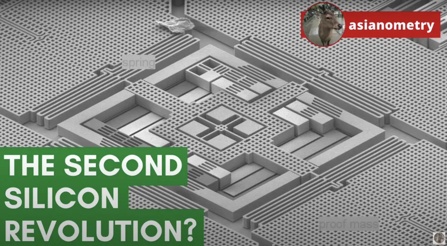
Imagine a tiny speaker as big as a microchip. Smaller than a penny and made entirely out of silicon. A speaker! That's the miracle of MEMS.
MEMS or Microelectromechanical Systems are microsystems with both electric and mechanical functions.
Built with the same advanced techniques that make today's integrated circuits, MEMS are everywhere around us.
The tech is miraculous but the industry has long struggled with several significant economic issues. In this video, we are going to look at the big problems with making small mechanical systems.
Beginnings
People have long dreamed of making things really, really small. In 1959, Richard Feynman gave a lecture at Caltech called "There's Plenty of Room at the Bottom". In it, he talked about directly manipulating atoms one by one to create useful tools.
He offered a prize of $1000 for the construction of a tiny motor capable of fitting in a cube 0.4 millimeters on each side.
The reward was claimed less than a year later by a Caltech engineer. The engineer however had made this little motor using conventional tools, which met the letter of the challenge - but not its spirit.
It was not until 1967 when Harvey Nathanson at Westinghouse used pre-modern micro-machining techniques to develop a new type of transistor: The resonant gate transistor.
About one millimeter long and made of gold, the special thing about this transistor was that it can move. Using electricity, researchers can control the distance between the gate and the electrode. Because it only responded to a narrow range of input signals, it was useful as a frequency filter - the first real MEMS product.
First Applications
It would not be until 1979 however when MEMS hit the big time. Hewlett-Packard used silicon micro-machining techniques to develop a printer inkjet nozzle to enable Thermal Inkjet Technology. Such nozzles would probably be the technology’s single most successful application up until then.
Inkjet technology works by first rapidly heating up ink to something like 100 degrees Celsius. This creates tiny bubbles, which pushes out the ink through a micro-machined nozzle onto the paper. When the bubbles collapse, it creates a vacuum that sucks in more ink.
The nozzles themselves aren't mechanical - they don’t move - but MEMS technology helped create them. And their tiny size allowed HP to put a whole bunch of them together in order to increase printer resolution.
Sensors in Airbags
Then in the 1990s, the MEMS industry discovered another major commercial use with sensors for acceleration, pressure and direction. Such sensors are useful in the industrial, medical, and electronics fields.
First is the automotive airbag sensor. I spoke about this in my video about automotive semiconductors. But the original airbag sensor was a mechanical device. Essentially balls in a tube. These was large, heavy, complex, and expensive - costing hundreds of dollars.
In 1991, Analog Devices created the first commercial acceleration MEMS sensor - less than 1 square centimeter large. It looks really cool, with a number of capacitive sense "fingers" about 60 microns deep. The fingers are attached to a mass which moves when acceleration happens. The touching fingers change their capacitive value, which then is sensed by the chip and relayed to the relevant ECU.
Analog Devices put this accelerometer and its accompanying electronics onto a single silicon chip - the ADXL-50. 50, because it was able to sense sudden accelerations of up to 50 Gs.
A complete monolithic acceleration monitoring system that is smaller, more reliable, and costs far less to make - $5 as opposed to the old system's $20 to $100 cost. These accelerometer sensors contributed to the widespread adoption of airbags in cars.
Your standard car has since incorporated dozens of MEMS-based sensor devices inside your anti-lock brakes, active suspension, navigation control, rollover detection, and so on. Over 60 million MEMS-based airbag sensors alone have been made and sold.
Pressure Sensors in Medicine
The pressure sensor would be the next big application of MEMS technology. They are used to monitor blood pressure in hospitals, connecting to a patient's intravenous line.
Early external blood pressure sensors cost over $600 and had to be sterilized and recalibrated for each reuse. The MEMS version cost a fraction of that - just $10, the majority of the cost going to the packaging - which made it disposable and far easier to use in the medical field.
Mechanically, they are quite simple. Using MEMS technology, you craft silicon into a thin membrane which serves as a diaphragm.
Then you take four small stress-sensitive polysilicon resistors or piezoresistors and place them along the diaphragm's edges.
The diaphragm is then suspended over a vacuum cavity to form an absolute pressure sensor.
When pressure occurs, it changes the silicon band structure and changes the resistivity of the crystal. This is sensed and the signals are delivered to the relevant parties.
Today, the medical MEMS-based sensor industry is worth over $6 billion, and blood pressure sensors make up the single largest piece of that.
Inertial Sensors, Consumer Electronics
Manufacturers eventually built on the initial pressure sensor and accelerometer designs to create a variety of versatile, low-power sensors. And these inertial MEMS-based sensors as they are called are inside all of today's hottest consumer electronics.
Take the Nintendo Switch. Inside the main console and controllers are ultra-low power inertial sensors with gyroscope and accelerometer capabilities - the STMicroelectronics SH627.
MEMS micromachining technologies are also used in other consumer electronics products like visual displays, optical switches, and more. The latter is pretty interesting - where micromirrors are used to redirect light from one optical fiber to another fiber.
Making MEMS
The idea behind most commercial MEMS production workflows is to use high volume IC techniques - like for instance, photolithography and etching - to add or remove layers on a 2D substrate until you produce a 3D shape.
However, there is no one-size-fits-all methodology for the industry. Thus, companies have tried other approaches to more economically produce and machine MEMS. For instance, electrochemical micromachining.
First introduced as a manufacturing technology for low-end PCB boards, ECM can create a MEMS by locally and selectively etching metals with an electrode tip.
Other micro-machining methods include laser beam machining, electrodischarge machining, and LIGA (Lithographie Galano- formung Abformung) - which stands for something I cannot pronounce.
Better machining costs are necessary, because it sets a high hurdle for payback and profit.
However, large-scale MEMS fabrication is just one part of the ecosystem. Others significantly contribute to cost and production issues: The design and the back end steps.
MEMS Design
So MEMS and integrated circuits have a whole lot in common. But it would be a mistake to link them too closely together. Fundamentally, there are some very clear differences between the two.
The first is in the design. Designing MEMS is pretty interesting and specialized. You can't just miniaturize things and expect it to work the same way.
For instance, the forces of friction are much stronger than inertia here. On one hand, tiny flow spaces are much more prone to fluid blockages. These have be to be ameliorated.
On the other, certain biochips can use electric fields to pump reactant around the chip. This is only possible with electro-osmotic effects that exist at a micro-meter scale.
Beyond that, there are fundamental philosophical differences between semiconductor and mechanical design.
VLSI revolutionized semiconductor design with a modular approach to large systems design.
In VLSI, you can build up entire systems and chips by combining parts from generic modules and standardized cell libraries. The library is designed independently from the product - most often in conjunction with the production process. Like TSMC and their nodes. This helps make sure the final product yields.
The mechanical design world does not have anything like this with the exception of standardized bolts, fasteners, pipe fittings, and paint. Those are made by subcontractors uninvolved with the final process. Instead, mechanical components have to accommodate weight, space, and energy restrictions tailored to the specific product.
And VLSI objects only have to do one thing - they process signals, usually logic. Mechanical objects on the other hand have to contain liquids, rotate, slide, or support loads - often all at once. And this makes mechanical design - MEMS included - extremely custom.
With all that being said, there are companies making CAD and design automation software suites for the MEMS industry. Examples include COVENTORWARE and IntelliCAD. These have contributed a great deal to helping MEMS designers better understand the microstructure design and its electromechanical behaviors.
MEMS Packaging
Testing and packaging are described as the back end of semiconductor production process - where you take the finished die and turn it into a chip for inserting into the final product. Unheralded, they are nonetheless vital.
Looking at typical pricing, the majority of the price for a MEMS-based sensor comes from the packaging - 75-80% of the final cost. Which is a big reversal from the situation for integrated chips.
For instance, let us look at a pressure sensor for something like the heating and ventilation market or HVAC.
An HVAC pressure sensor is typically priced at about $20 to $30. The majority of that comes from the packaging rather than the actual die. A raw working die from a foundry without its packaging - and unusable by the way - costs less than 50 cents a piece.
The issue is fundamental and philosophical. An IC is a system in of itself. Thus, packaging serves a secondary support role - protecting it and interfacing it with the outside world.
So most of the time, you put it into a plastic or ceramic case.
MEMS on the hand, has to intimately interact with the outside world. You cannot throw a MEMS pressure sensor into a hard plastic case. How is it going to sense the pressure?
The packaging for each MEMS die has to be remade for its particular circumstances. A pressure sensor MEMS needs different packaging than a micro-mirror array. A microfluidic MEMS, different from an electrostatic actuator. So on. This adds substantial cost and engineering cost to the work.
A Little Economic Problem
As I mentioned, Analog Devices was one of the first major semiconductor companies to invest in the MEMS world with their miniaturized accelerometer.
The company started researching the space in the 1980s, specifically targeting the airbag sensor industry. They built their own in-house manufacturing facility to scale up production.
But it took nine years for that facility to come into the black. The problem was pricing. From the very start, Analog Devices marketed their product as having a significant price advantage over the competition.
So when Analog signed its first automotive sensor deal with Siemens for its MEMS products, they had to build in automatic price declines over the next six years from $11 per unit to $6.
Analog did this because they thought they could get more efficient on production. Much like for the IC industry, yield is the single biggest influencing factor for product cost. A 10% yield means that 9 out of 10 MEMS products are not usable.
Doubling the yield means halving the cost, but this is not exactly easy to achieve. Which leads to overly optimistic projections of what's possible, and market prices that do not reflect the actual investment put into the whole process: Development, production, packaging and testing.
Relentless market price erosion - as high as 3-5% each quarter - eats away at margins, and disincentives investment into other potentially exciting possibilities for the MEMS industry.
For instance, micro-propulsion technologies for small cube satellites.
Or MEMS-based LIDAR mirrors for autonomous cars.
Or IOT sensors - whatever those might end up being. And so on.
Conclusion
MEMS has been called the second silicon revolution. And it is still magic. You are talking about microscopic moving parts that can do the same things as much larger things. They are smaller, cheaper, and work better. That's magical.
But the industry has partially been the victim of its own success. Its creativity and diversity make it harder to come towards a widespread standard. And MEMS has nothing like a SEMATECH or a DARPA working within the industry to map a way forward.
I reckon that for the industry to realize its full technical and commercial potential that the various players - the fifty some designers, foundries, vendors, and end users all about - need to start working together more closely to make standards and find solutions to the underinvested issues that plague it.
©2026 Business Next Media Corp. All Rights Reserved. No.102, Guangfu S. Rd., Da'an Dist., Taipei City 106, Taiwan