©2026 Business Next Media Corp. All Rights Reserved. No.102, Guangfu S. Rd., Da'an Dist., Taipei City 106, Taiwan
Semicon Taiwan 2023: What tech giants think of the future of Silicon Photonics
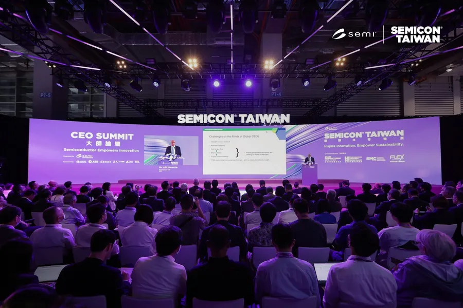
Top semiconductor companies are actively working on silicon photonics, muscling to win this critical battle by keeping up with Moore’s law. During the annual semiconductor event Semicon Taiwan 2023, companies gathered to share insights into how silicon photonics will boost AI applications, and how this technology evolves.
As the curtains close on Semicon Taiwan 2023, the world's semiconductor industry collectively exhales. Semicon Taiwan 2023 shattered all previous records, boasting a staggering number of participants and exhibitions. With over 950 leading companies from 10 different countries converging at the event, and more than 3,000 booths brimming with cutting-edge technologies, this exhibition unequivocally cemented its status as Taiwan's largest annual semiconductor gathering.
Among all the panels and sharing, silicon photonics is one of the most heated topics and also the opening theme for the grand event. Top semiconductor companies shared their views and progress on silicon photonics technologies, stressing its importance in the field.
To keep up with Moore’s Law, silicon photonics plays an important role, says TSMC
It’s not a new term for the semiconductor industry. Brought up by Intel in around 2015, silicon photonics refers to using silicon as a special material for optical systems. Silicon is carefully shaped into tiny components that work with light, particularly in the infrared range, which is widely used in fiber optic communication. This integration of optics and electronics on a single chip holds the promise of faster data transfer, contributing to the ongoing quest to keep up with Moore's Law.
“To accelerate the AI applications, silicon photonics is the key in the semiconductor industry,” said Mark Liu, executive Chairman of Taiwan Semiconductor Manufacturing Company (TSMC). In the realm of high-performance computing, comprised of numerous chips executing large AI models, the velocity of wired communication channels is swiftly becoming a bottleneck for computational speed. Presently, optical interconnects are already being employed to link servers within data center racks. Optical interfaces are coupled with Graphics Processing Units (GPUs) and Central Processing Units (CPUs), promising to supply energy-efficient and bandwidth-expanding communication among GPUs. Consequently, hundreds of servers may coalesce into a single massive GPU, unified by a shared Dynamic random-access memory (DRAM).
TSMC’s current technology Compact Universal Photonic Engine (COUPE) plays a critical role in the development of silicon photonics, according to Liu. COUPE is a photonic processing system that combines photonic components into a single compact unit, which makes it a powerful tool for optical signal processing, communications, and other photonics-related tasks. Leveraging System on Integrated Chip (SoIC) technology, COUPE seamlessly integrates Integrated Circuits (EIC) and Photonic Integrated Circuits (PIC) adjacent to GPUs and router switches.
Driven by the demands of AI applications, silicon photonics technology is becoming the linchpin of the semiconductor industry. Now, data transfer between microchips mainly relies on telecommunications, while silicon photonics can bust through the bottlenecks by making it faster and less energy consumption. The advantage of a COUPE lies in its ability to perform multiple functions with high precision and speed, often surpassing what traditional electronic circuits can achieve.
Some big names in the field like ASE, Cisco, and Advantest also gathered to discuss the latest developments in silicon photonics. “If you want to support faster and better communication between AI and edge devices, you will need a photonic integrated circuit (PIC),” according to Tien Wu, CEO of ASE. A photonic integrated circuit (PIC) or integrated optical circuit is a microchip containing two or more photonic components that form a functioning circuit.
“The real optical challenge, lies in the costs of the test,” said Daisuke Watanabe, executive officer at Advantest, the leading manufacturer of automatic test and measurement equipment used in the design and production of semiconductors for applications. The cost of photonic testing today takes up more than 10% of the average selling price (ASP), which has been a major cost factor for photonic devices, according to Watanabe. Industry standardization, innovation to ease fiber alignment, and commercially available optical automatic test equipment modules are required for further development.
There is no doubt that top semiconductor companies are actively working on silicon photonics, muscling for market shares. Wu highlighted that ASE has already integrated silicon photonics technology into various facets of its offerings, including Co-Packaged Optics (CPO) products, artificial intelligence, and machine learning chips. Furthermore, in the domain of 3D optical technology and Lidar applications, ASE is actively engaged in developing integrated solutions that combine metasurface lenses (metalenses) with silicon photonics packaging techniques.
On the other hand, TSMC is reportedly collaborating with major clients such as Broadcom and NVIDIA on joint development efforts. They are expected to receive significant orders as early as the second half of next year, with TSMC deploying a dedicated research team of over 200 experts for this endeavor.
Three waves of silicon photonics
In 2015, Intel came up with silicon photonics, a new concept for the next generation of chips. Since then, three waves of silicon photonics have occurred, driven by the quest for faster and more efficient communication technologies. Silicon photonics has been on a steady ascent, with applications ranging from data center interconnects to high-speed communications and even emerging fields like Light Detection and Ranging (Lidar) for autonomous vehicles and mobile device sensors.
Tien Wu, CEO of Advanced Semiconductor Engineering, ASE, emphasized the pivotal role of silicon photonics in advancing various technological frontiers. He highlighted the three waves driving silicon photonics' evolution.
The first wave focuses on networking with optical transceivers, offering substantial power savings of up to 30%. In the second wave, silicon photonics enters the realm of computing with optical I/O, which is an optical interconnect integrated into the same package as compute chips. It starts to serve applications like AI and machine learning, enabling remarkable power savings of 50% while simultaneously increasing bandwidth by 10%.
The third wave introduces 3D optics with Optical Phased Arrays (OPA), which have applications in LIDAR systems and mobile device sensors. This progression underscores the critical role of photonic integrated circuits (PICs) in enabling faster and more efficient communication between AI systems and memory or edge devices. Furthermore, Tien Wu discussed the need for a different ecosystem to accommodate photonic Original Design Manufacturers (ODMs) and Original Equipment Manufacturers (OEMs). As new technologies spring up, the next wave is certainly around the corner.
©2026 Business Next Media Corp. All Rights Reserved. No.102, Guangfu S. Rd., Da'an Dist., Taipei City 106, Taiwan